
P25N10H
P25N10H is a Serial Multi I/O NAND Flash Memory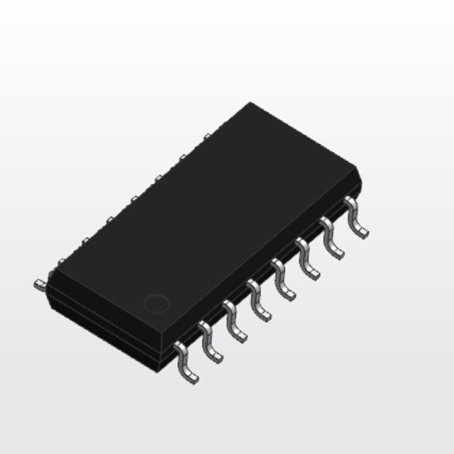
 P25N10H.PDF
 …ΧΤΖ–≈œΔ
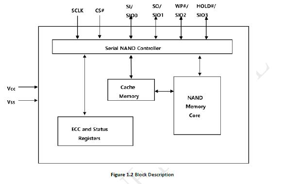
The P25N10H is a 128Mx8bit with spare with spare 4Mx8 bit capacity. The device is offered in 3.3 Vcc Power Supply, and with SPI interface. The memory is divided into blocks that can be erased independently so it is possible to preserve valid data while old data is erased.
Features
1. 1Gbit NAND Flash Memory
- Page size: 2048 bytes page for read and program, spare 64 bytes
- Block size: 64 pages (128K+4K bytes)
- Device size: 1 Gbit (1024 blocks)
2. Single 3.3 Volt core supply
3. Industrial Temperature Range - 40 °C to 85°C
4. Serial Peripheral Interface (SPI) Compatible: Mode 0 and Mode 3
5. Single, Dual, Quad SPI, QPI
- Standard SPI: SCLK,CS#,SI,SO,WP#,HOLD#
- Dual SPI: SCLK,CS#,IO0,IO1,WP#, HOLD#
- Quad SPI: SCLK,CS#,IO0,IO1,IO2,IO3
6. Advanced Security Features
- Write protect all/portion of memory via software
- Hardware controlled locking of protected sectors by WP pin
- 48 Kbyte One Time Programmable (OTP) region
7. High Performance
- 104 MHz for fast read with 30pF load
- Latency of array to register: 25us maximum
- Quad I/O Data transfer up to 416Mbits/s
8. Fast Program and Erase Speed
- 300us typical page program time
- 2ms typical block erase time
9. Enhanced access performance
- 1Kbyte cache for fast random read
- Cache read and cache program
10. Advanced Feature for NAND
- Internal data move by page
- The first block (Block0) is guaranteed to be a valid block at the time of shipment.
11. High Reliability
- 50,000 Program / Erase Cycles (with 4bit ECC)
- 10 - year Data Retention
12. Industry Standard Green Package Options
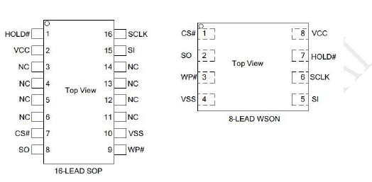
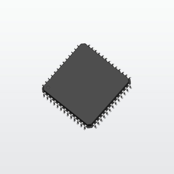
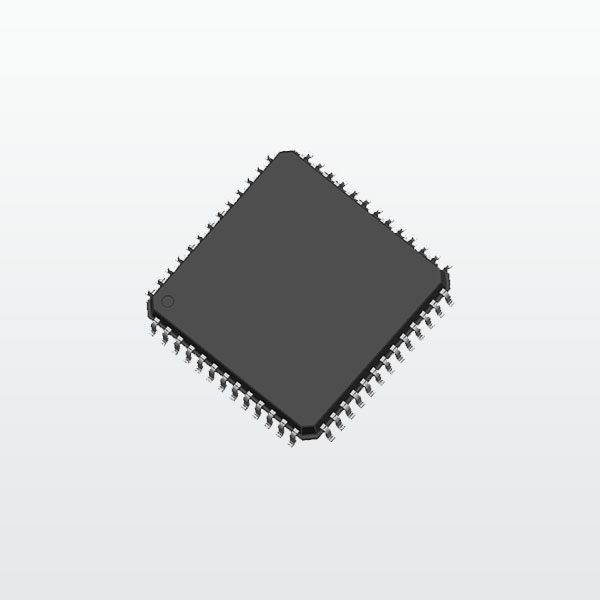
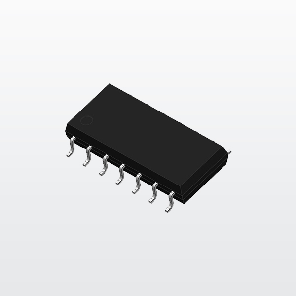
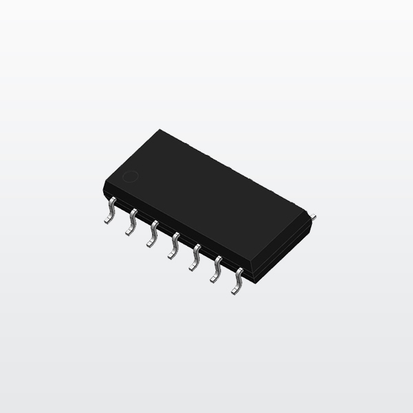
- 16 - pin SOP (300mil)
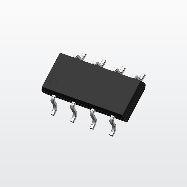
- 8 - land WSON (8x6mm)
P25N10H’s Block Diagram
P25N10H’s Package
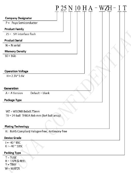
P25N10H’s Ordering Information
»γΚΈΙΚ¬ρ
‘ΎœΏΉ…―·
Ϋ®“ιΝψ έΦέΗώΫω”Ο”Ύ‘ΛΥψΘ§“‘‘ΣΈΣΒΞΈΜΘ§≤Δ«“ΦέΗώ «ΗΓΕ·ΒΡΓΘ »τ“Σ≤ι―·”–ΙΊ≈ζΝΩΦέΗώΓΔ±ΨΒΊΜ豓ΦέΗώΜρΫΜΗΕ±®ΦέΒΡ–≈œΔΘ§«κ”κΙΪΥΨΝΣœΒΓΘΘ®ΒψΜςΉ…―·Θ©
ΒψΜς’βάοΗχΈ“ΖΔœϊœΔΝΣœΒΖΫ Ϋ
“ΒΈώΒγΜΑΘΚ0755/23141725 18576699326
“ΒΈώQQΘΚ2335804557¥Ϊ’φΘΚ0755/23141201
QQΘΚ2286874832Θ®ΖΫΑΗΘ© 1762516767Θ®ICΘ©
” œδΘΚsunnyqi001@126.com
ΒΊ÷ΖΘΚ…νέΎ –±ΠΑ≤«χΈςœγ–¬Κΰ¬Ζ”κάΆΕ·¬ΖΫΜ≤φΩΎ±ΠΫίΑ≤Ψ≠Ο≥÷––Ρ503Θ®¬ό±ΠœΏΤΚ÷όΒΊΧζ’ΨB≥ωΩΎΘ©
ΙΪΥΨΙΌΆχΘΚhttp://www.sunnyqi.com/
―υΤΖΦΑ―·Φέ
Ϋ®“ιΝψ έΦέΗώΫω”Ο”Ύ‘ΛΥψΘ§“‘‘ΣΈΣΒΞΈΜΘ§≤Δ«“ΦέΗώ «ΗΓΕ·ΒΡΓΘ »τ“Σ≤ι―·”–ΙΊ≈ζΝΩΦέΗώΓΔ±ΨΒΊΜ豓ΦέΗώΜρΫΜΗΕ±®ΦέΒΡ–≈œΔΘ§«κ”κΙΪΥΨΝΣœΒΓΘΘ®ΒψΜςΉ…―·Θ©
έΚσΖΰΈώ
…ΘΡαΤφΩΤΦΦ «…νέΎ –÷ΣΟϊΒΡIC¥ζάμ…ΧΘ§ΡήΈΣΙψ¥σΙΛ≥Χ Π”κ≤…ΙΚ≈σ”―ΧαΙ©÷ΎΕύάύ–Ά≤ζΤΖΘ§–Γ≈ζΝΩΒ±ΧλΫΜΜθΘ§10K“‘…œ5-10ΧλΫΜΜθΓΘ
œύΙΊ≤ζΤΖ


- ΩΆΖΰ»»œΏΘΚ
0755-23141725 -
IC≤ζΤΖΉ…―·
-
ΖΫΑΗΉ…―·
- …νέΎ –…ΘΡαΤφΩΤΦΦ”–œόΙΪΥΨ
- “ΒΈώ»»œΏ: Υοœ»…ζΘΚ18576699326/ QQ:2335804557 ¥Ϊ’φΘΚ86-0755-23141201 ” œδΘΚsunnyqi006@126.com
-
’Ϋ¬‘ΚœΉςΦΑ≤…ΙΚ»»œΏ:
Υοœ»…ζΘΚ13510901648/ QQ:2361879025
 “ΒΈώΈΔ–≈
 ’Ϋ¬‘ΚœΉςΈΔ–≈